3D printed circuit boards are revolutionizing the way we design and manufacture electronic components, offering unprecedented flexibility and efficiency. With advancements in printed circuit board technology, companies like Nano Dimension are at the forefront of this innovation, providing tools such as the Dragonfly 2020 desktop 3D printer to create intricate circuit board prototypes rapidly. This groundbreaking printer can reduce the development timeline from weeks to mere hours, enabling engineers and designers to iterate their projects with remarkable speed. Employing advanced inkjet-like deposition methods and nano-inks, the Dragonfly 2020 produces reliable multi-layer PCBs that meet the demands of modern electronics. As this technology evolves, the potential for in-house production could transform the entire landscape of PCB manufacturing, presenting significant advantages for industries ranging from healthcare to electronics.
Advanced manufacturing techniques such as additive manufacturing for electronic components are gaining traction, particularly through innovations like the Dragonfly 2020 by Nano Dimension. This desktop 3D printer specializes in the creation of multi-layer circuit board prototypes, presenting a new frontier in PCB design and production. The implications of such innovations are profound; they promise faster turnaround times and customizable solutions that traditional PCB manufacturing processes cannot match. Driven by materials optimized for conductivity and insulation, this technology exemplifies a shift toward more efficient and localized production methods. As various sectors explore these state-of-the-art circuit board solutions, the future of electronics manufacturing is set to become more dynamic and accessible.
The Evolution of 3D Printed Circuit Boards
In recent years, the advancement of 3D printed circuit boards (PCBs) has transformed the electronics manufacturing landscape. With companies like Nano Dimension leading the charge, the potential for on-demand PCB production has become a reality. The Dragonfly 2020, a desktop 3D printer developed by Nano Dimension, allows users to create complex multi-layer circuits in a matter of hours, drastically reducing the time typically required for prototype development. This innovation is particularly beneficial for industries that rely on rapid iterations and testing, enabling companies to bypass traditional outsourcing in favor of in-house production.
The significance of 3D printed circuit boards extends beyond mere speed; they also offer unique advantages in terms of customization and efficiency. Nano Dimension’s technology allows for the printing use of conductive silver inks and dielectric materials in one process, enabling the creation of PCBs with intricate designs that are not feasible with conventional manufacturing techniques. This ability to integrate multiple functionalities into a single board can lead to unique product identity and can enhance performance by optimizing the layout of electronic components.
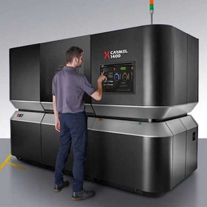
Understanding the Benefits of the Dragonfly 2020
The Nano Dimension Dragonfly 2020 represents a groundbreaking shift in how circuit board prototypes are developed. By employing an innovative inkjet-like material deposition method coupled with a heat-based curing system, the printer ensures a high level of precision and quality in the final product. According to Amit Dror, the co-founder and CEO of Nano Dimension, this method allows for multiple layers to be created without physical limitations, making it easier than ever for designers to experiment with complex circuit configurations that suit their needs.
Additionally, the Dragonfly 2020 opens new opportunities for manufacturers to protect their intellectual property. With the traditional PCB manufacturing process often reliant on external vendors in regions such as Asia, creating prototypes in-house enables companies to maintain confidentiality over their designs and ideas. This localized approach not only speeds up the prototyping process but also fosters a culture of innovation, as engineers can iterate designs quickly based on real-time feedback.
Breaking Down the Challenges of Current PCB Technologies
Despite the significant advancements represented by 3D printed circuit boards, there are still notable challenges to overcome in the wider adoption of this technology. Industry experts acknowledge that while printing PCBs using multiple materials is a remarkable achievement, complexities remain in balancing speed, cost, and material behavior during the printing process. Ensuring that the materials used can withstand the heat and stress they will encounter in real-world applications is critical to the success of any PCB printed with the Dragonfly 2020.
Moreover, manufacturers still need to tackle production volume challenges. The current capabilities of 3D printed circuit boards are ideally suited for prototypes or small batch runs, yet the demand for large-scale production remains unmet. To achieve this, scaling the technology while managing costs effectively will be paramount. Industry leaders believe that ongoing research and advancements in 3D printing and printed circuit board technology will address these issues, potentially unlocking significant market growth and expansion.
The Future of Desktop 3D Printers in Circuit Board Manufacturing
As the demand for more integrated electronic systems continues to rise, the future of desktop 3D printers like the Dragonfly 2020 appears promising. The adaptability of these printers allows for the production of custom circuit board prototypes tailored to specific applications, fostering innovation across various sectors, including healthcare, defense, and consumer electronics. The ability to rapidly prototype small production runs means businesses can bring products to market faster while minimizing risks associated with new designs.
Furthermore, as more companies begin to adopt this technology, we may see an increase in collaborations and partnerships that drive further innovation in PCB manufacturing. Companies are likely to explore new materials and techniques, which could ultimately lead to enhanced performance, reliability, and cost savings in the production of 3D printed circuit boards. Engaging with industries that span electrical, mechanical, and software design will pave the way for further advancements, making desktop 3D printers an integral part of the modern manufacturing landscape.
Collaborative Efforts in PCB Development
Nano Dimension’s approach to collaboration with beta customers, including banks, healthcare companies, and defense contractors, highlights the importance of cross-industry partnerships in advancing PCB technology. By working closely with these diverse organizations, Nano Dimension can gather valuable insights and feedback that drive further improvements and tailor their technology to meet specific industry needs. These partnerships not only enhance the capabilities of their 3D printing systems but ultimately lead to innovative applications of printed circuit boards.
Moreover, collaboration within the industry serves to broaden the understanding and applications of 3D printed circuit boards. Engaging with experts from various sectors allows for knowledge sharing that could lead to the development of bespoke solutions for common challenges in PCB design and manufacturing. As the complexities of modern electronics continue to evolve, the collaborative culture fostered by companies like Nano Dimension will be crucial for achieving the next breakthroughs in circuit board technology.
Market Trends in PCB Technology
As of late, the printed circuit board (PCB) market is experiencing a transformative period, driven by technological innovations like those demonstrated by Nano Dimension and their Dragonfly 2020. Analysts predict steady growth, with the market anticipated to move from a valuation of $63.5 billion in 2016 to an estimated $73.8 billion by 2021. This growth indicates a robust demand for advanced PCB solutions and underlines the necessity for companies to adapt to new printing technologies to maintain competitive advantage.
The increasing trend of in-house PCB prototyping promises to reshape established manufacturing paradigms. With firms seeking faster turnaround times for circuit board prototypes, the availability of desktop 3D printers will likely lead to a shift away from conventional outsourcing strategies. This transition not only benefits time efficiency but also improves design security, permitting companies to innovate without the fear of intellectual property theft—a significant concern in a highly competitive global market.
Comparing Nano Dimension with Competitors
While many companies have ventured into the realm of 3D printed circuit board technology, few have made as significant an impact as Nano Dimension with their Dragonfly 2020. Competitors like Voltera and Voxel8 have developed their own systems, each with unique features and functionalities. However, Nano Dimension’s ability to print both dielectric and conductive materials in high resolution stands out, offering advantages in the complexity and durability of the final product.
The competitive landscape for 3D PCB printers suggests a growing focus on innovation and specialization. As companies strive to differentiate themselves, the battle for market share will rely heavily on the effectiveness of their technologies and the versatility they can offer to consumers. Nano Dimension’s early establishment in the market gives it a strategic advantage; however, continued innovation and adaptation will be crucial to maintaining a leading position as new entrants emerge.
The Role of Customization in PCB Design
Customization has become an increasingly vital aspect of PCB design, enabling companies to tailor their products to meet specific market demands. With the help of 3D printing technology, particularly through systems like Nano Dimension’s Dragonfly 2020, designers can create unique circuit configurations that were previously challenging or impossible to achieve. This level of customization not only enhances functionality but also allows for aesthetic considerations that align with branding and consumer preferences.
Moreover, the ability to quickly adapt designs on the fly accelerates the development process. As consumer electronics become more sophisticated, the demand for specialized components that fit unique shapes and functions grows. The customization capabilities of 3D printed circuit boards cater directly to this trend, ensuring that manufacturers can stay agile and responsive to changing market needs. As this technology matures, the possibilities for creative and effective use of custom-designed PCBs will expand significantly.
Technological Advancements on the Horizon
Looking ahead, the field of 3D printed circuit boards is poised for remarkable advancements. Innovation is not just limited to the printer’s capabilities but also encompasses the development of new materials and techniques that enhance the performance of printed circuit boards. There is vast potential to explore functional inks and substrates that can contribute to better thermal management, conductivity, and flexibility, thereby opening the door for entirely new applications.
In addition, the integration of AI and machine learning algorithms in PCB design and printing could revolutionize the industry, enabling more intelligent and adaptive manufacturing processes. As the understanding of materials science deepens, the potential for creating highly specialized, efficient, and sustainable circuit board solutions will become increasingly attainable. Such developments will undoubtedly shape the future of electronics manufacturing, making 3D printed circuit boards a pivotal element in the evolution of technology.
Frequently Asked Questions
What are 3D printed circuit boards and how do they work?
3D printed circuit boards (PCBs) are layers of insulating material and conductive pathways manufactured using advanced 3D printing technology. The process typically involves a machine like Nano Dimension’s Dragonfly 2020, which uses inkjet-like material deposition methods to lay down dielectric and conductive materials in multiple layers. This allows for rapid prototyping, enabling developers to create circuit board prototypes and small production runs in a matter of hours instead of weeks.
What advantages do 3D printed circuit boards offer over traditional manufacturing methods?
3D printed circuit boards, such as those produced by Nano Dimension’s Dragonfly 2020, offer numerous advantages including significantly reduced development times, enhanced customization possibilities, and the ability to keep intellectual property secure by manufacturing prototypes in-house. Additionally, the technology allows for complex designs that can integrate custom features and mitigate the risk of counterfeiting.
How does Nano Dimension’s Dragonfly 2020 enhance printed circuit board technology?
The Dragonfly 2020 enhances printed circuit board technology by utilizing an innovative material deposition method that combines dielectric insulating materials with silver-based nano-inks. This allows it to print multi-layer circuit boards with intricate circuitry at high resolution, where conductive traces can be as narrow as 100 microns. It also facilitates rapid design modifications in a shorter timeframe, greatly benefiting prototyping processes.
What is the expected cost of the Dragonfly 2020 3D printer for circuit board production?
The Nano Dimension Dragonfly 2020 3D printer is expected to retail for approximately $200,000 when commercially available. This initial investment offers significant cost savings in the long run for companies looking to prototype and produce unique printed circuit boards internally.
Who are the current users of Nano Dimension’s 3D printed circuit board technology?
Currently, Nano Dimension is collaborating with 10 beta customers, which include major sectors such as banking, healthcare, defense, and electronics. These organizations are testing the Dragonfly 2020’s capabilities to enhance their prototyping and manufacturing processes, under confidentiality agreements preventing the disclosure of specific names.
What materials can be used in 3D printed circuit boards with the Dragonfly 2020?
The Dragonfly 2020 can utilize a combination of dielectric insulating materials and conductive silver-based nano-inks to create printed circuit boards. It successfully prints two types of materials, which can withstand high temperatures and are essential for producing high-resolution electrical pathways. This dual material capability sets it apart in the PCB manufacturing landscape.
How does 3D printing change the way circuit board prototypes are developed?
3D printing revolutionizes the development of circuit board prototypes by enabling rapid iteration and modification of designs directly in-house. Instead of waiting weeks for traditional fabrication, users can create and test new circuit board designs within hours using machines like the Dragonfly 2020, significantly speeding up the overall development cycle.
What future advancements can be expected in the field of 3D printed circuit boards?
In the future, advancements in 3D printed circuit boards could include improvements in printing speed, cost-efficiency, and the ability to utilize multiple materials simultaneously. As technology evolves, it is anticipated that 3D printing will further integrate into the production of electronics, leading to more sophisticated and adaptable circuitry designs that align closely with device specifications.
| Key Feature | Details |
|---|---|
| 3D Printer Model | Dragonfly 2020 |
| Company | Nano Dimension |
| Production Capability | Multi-layer circuit boards |
| Development Time Reduction | From weeks to hours |
| Materials Used | Dielectric materials and silver-based nano-inks |
| Key Technology | Inkjet-like material deposition and heat-based curing |
| Conductive Trace Width | Approximately 100 microns |
| Expected Price | $200,000 |
| Market Growth | Projected to reach $73.8 billion by 2021 |
| Research Insights | Potential for custom products and counterfeiting challenges |
Summary
3D printed circuit boards represent a groundbreaking leap in prototyping technology. With the introduction of devices like Nano Dimension’s Dragonfly 2020, companies can significantly reduce the time it takes to develop circuit board prototypes—from weeks to mere hours. This advancement not only fosters innovation but also enhances the security of intellectual property by allowing for in-house prototyping. As the market for these boards continues to grow, the potential for scalability and unique design capabilities presents enticing opportunities for industries ranging from electronics to healthcare.
Related Posts

3D Printing: Unleashing Creativity with ARKit and Obsidian
3D printing is revolutionizing the way we create and interact…
Metal 3D Printer: A World-First Trial by the Royal Australian Navy
Metal 3D printers are revolutionizing the landscape of manufacturing, particularly…

3D Printer Ratings: Top Machines in 2017 Revealed
When it comes to choosing the right 3D printer, understanding…